


Table of contents
PCB assembly cost drivers include board size, drill holes, materials, layers, and design complexity. Understanding how each component affects costs can help create a cost-effective PCB design.
No electronic device will function without components, and the components you choose will likely be the biggest cost driver for your device. One nasty surprise that new designers might receive when putting a board into assembly is an unexpectedly high cost for assembly based on the use of certain component packages. If you use components in certain packages your production costs could be higher than you expected.
What’s problematic about this is its relation to design to cost. If you get through the design phase with cost-boosting components and they aren’t included in your budget, you might have trouble hitting your per-board production costs at your target volume. So if you have a strict cost target, but you want to slash as much as possible from your board assembly costs, make sure you know which packages will create assembly cost increases.
Which Packages Cost More to Assemble?
There are a few packages that cost more to assemble, or that can create more cost when used double-sided. These are outlined in the sections below. In a basic sense, the machine time cost for assembling these parts is the same as any other part. The additional cost comes from additional inspection requirements, potential difficulties in developing test fixtures, and additional reflow passes.
Leadless Parts (BGAs, LGAs, and QFNs)
A part that comes in a BGA package will always cost more to assemble than the same part in a non-BGA package. This applies regardless of pin count or the size of the package, and the same applies to LGA packages and QFN components, the latter of which applies to many ASICs.
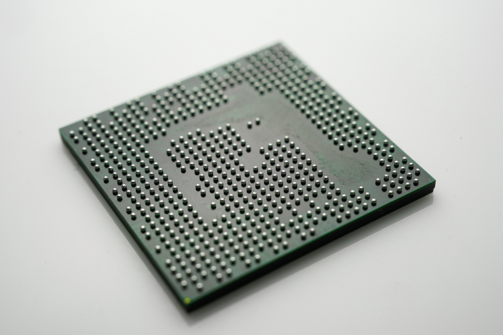
Why would this be the case? Both package types mount to pads or via-in-pad directly on the PCB surface. This leaves the pads concealed beneath the package, so they cannot be inspected with automated optical inspection (AOI). The additional cost comes from additional X-ray inspection requirements, which requires a skilled operator and machine time on an X-ray imaging unit.
There could also be additional costs from in-circuit testing requirements, assuming this is part of your assembly order needs. Testing with BGAs requires via holes to be exposed on the back side of the BGA region. In some BGAs, these points won’t be available if blind/buried vias are used, so only passives mounted on the back side can be exposed or other parts in the board need to be probed. This could increase NRE costs for the board to ensure accurate inspection.
Overlapping BGAs at Volume
Double-sided assembly always costs more than single-sided assembly. The reason for this is simple: an additional reflow pass is required to mount parts onto the board. As long as we are not dealing with something like overlapping BGAs, double-sided assembly is a modest increase in per-board costs. Soldering BGAs on both sides of the board can incur additional costs, but you may not see the costs arise until you are assembling at high volume.
The quality and yield issue that can arise from double-sided BGA assembly can be handled in low volume assembly. At high volume, you may see greater NRE and/or additional per-board cost depending on how the BGAs are arranged; this will become more of a challenge as more parts are supplied in micro-BGA packaging. When there are overlapping BGAs, the following process can be used:
- The side with the smaller overlapping BGAs is assembled first
- The first reflow pass can be inspected to specifically isolate that BGA
- The side with the larger BGA is assembled second and inspected
This order is preferred as the smaller BGA will have a lower chance of desoldering during the second reflow pass. However, it increases the processing steps and thus impacts cost. Boards for these systems also cost more regardless; overlapping BGAs can’t use through-holes for fanout, so they must have high layer count HDI boards that are already expensive.
To solve this, you have two options: swap a BGA for a leaded package, or arrange them so that they do not directly overlap. Both cases remove the need for additional steps in assembly. If you opt for a leaded package instead of a micro-BGA you get the most cost benefit as those components can be verified with AOI rather than X-ray inspection.
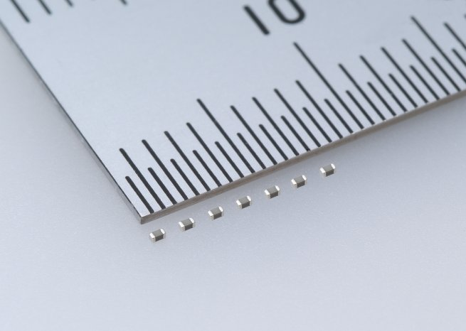
0201 or Smaller Passives
Very small passives are great for saving space, but they can carry higher costs with some assemblers. These very small passives can typically carry higher attrition requirements because they are easier to lose during production, and a lost part requires pulling from another part from a reel.
These points don’t just apply to passive components, they also apply to parts that come in equivalent package sizes. Some assemblers will not make a distinction between standard passives (resistors, capacitors, and inductors), but others will demand that any component in these equivalent case sizes carry higher costs as well as higher attrition requirements. Make sure to read your assembler’s attrition and kitting requirements to ensure you account for these cost factors.
Spot Alternative Packaging Early
For some parts, you won’t have any choice but to use a part with a BGA or QFN package. This is definitely the case with certain application processors, more advanced ASICs, and large FPGAs. But if you can get visibility into package alternatives early, you have the option to swap for a lower cost part that has equivalent functions. These alternatives could be:
- Pin-equivalent direct substitutes from a different manufacturer
- Alternative MPN in the same part family
- Functionally equivalent part without pin equivalence
All of these cases are much easier to deal with after your design is engineered, but before you start the PCB layout. So before you dive head-first into your PCB, make sure you reduce your cost risk and source your parts with a logistics platform like Cofactr.